| |
|
|
 |
| |
| PCB Product |
| |
Multech PCB Technologies Co., Limited has been specialized in manufacturing printed circuits for more than 22 years. Multech has abundant experience of making PCBs and perfect management mechanism. Multech is a PCB supply specialist and strongly
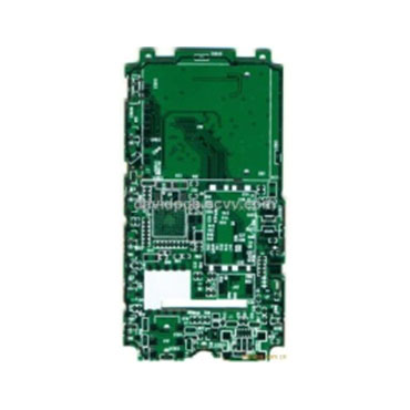
A printed circuit board, or PCB, is used to mechanically support and electrically connect electroniccomponents using conductive pathways, tracks or traces etched from copper sheets laminated onto a non-conductive substrate. It is also referred to as printed wiring board (PWB) or etched wiring board. A PCB populated with electronic components is a printed circuit assembly (PCA), also known as a printed circuit board assembly (PCBA).
PCBs are inexpensive, and can be highly reliable. They require much more layout effort and higher initial cost than either wire-wrapped or point-to-pointconstructed circuits, but are much cheaper and faster for high-volume production. Much of the electronics industry's PCB design, assembly, and quality control needs are set by standards that are published by the IPC organization.
|
|
Product |
|
+ Flex-Rigid PCB
+ flexiblePCB
+ Single sided and Double sided PCB
+ flexPCB
+ HDI PCB
+ HeavycopperPCB
+ Multilayer PCB
+ SingleAluminiumPCB
+ Single side and Double sided PCB
+ BlindviasPCB |
|
|
|
| |
|
| |
| |
|
|
|
|
|
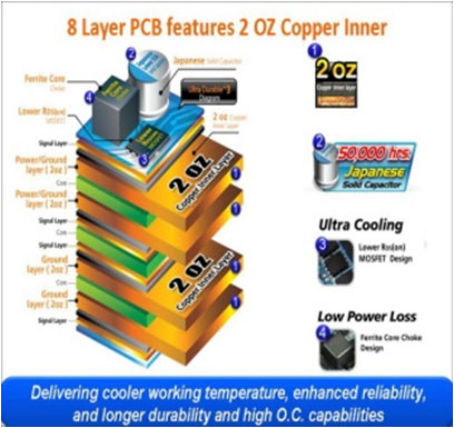
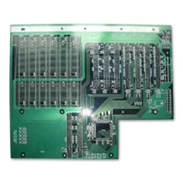
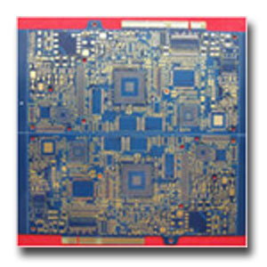
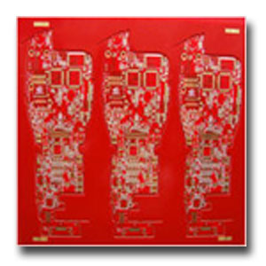
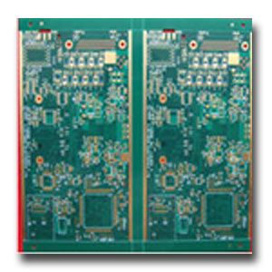
8-layer PCB that comes with ENIG finish. The product has HASL, lead-free HASL, OSP, immersion silver or tin, carbon ink, and selective gold surface treatment. It is also gold plated via electrolysis. |
|
|
|
| |
 |
 |
Technological requirements
Layer:8 layer
Material:FR4
Thickness:1.0mm
Flash: ENIG
Min. hole size:0.1mm(4mil)
Min. line width:0.1mm(4mil)
Min. line space: 0.1mm(4mil)
Special: Blind & buried +Impedance control
Seal package |
|
| |
|
|
|
| |
|
| |
Other products from this company
|
|
| |
|
| |
|
|
| |
|
4 layer
P/N:P4C3687A
layer:4
Board thickness:1.6mm
Surface Finishing:Immersion Gold
size:180mmX215mm
copper thickness:H/1/1/H
conductor width/ spacing : 5mil/5mil
hole diameter : 0.30mm: |
|
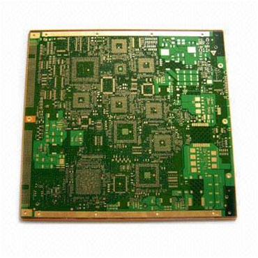
8 layer
P/N:P8C5441A
Layer :8
Board thickness :1.6mm Surface Finishing :Immersion Gold size:50mmX230mm
copper thickness :H/1/1/H
conductor width/ spacing : 6mil/6mil
hole diameter :0.40mm: |
| |
|
|
|
|
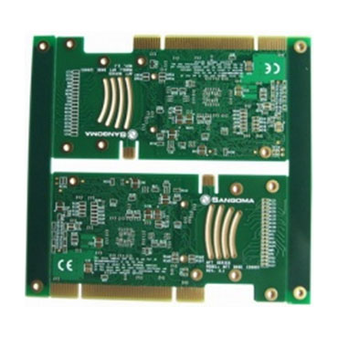
10 layer
P/N :P10C3481A
Layer :10
Board thickness :1.8mm
Surface Finishing :Immersion Gold size:180mmX253.3mm
copper thickness :1/1/1/1/1/1/1/1/1/1oz
conductor width/ spacing : 5mil/5mil
hole diameter : 0.30mm: |
|
4 layer
P/N : P4C4673A
Layer :4
Board thickness :1.6mm
Surface Finishing :Immersion Gold size:180mmX210.5mm
copper thickness :H/Hoz
conductor width/ spacing : 5mil/5mil |
hole diameter : 0.20mm |
| |
|
|
|
|
2 layer
P/N :P2E3457A
Layer :2
Board thickness :1.6mm Surface Finishing :OSP
size::80mmX170mm
copper thickness :1/1oz
conductor width/ spacing : 5mil/5mil
hole diameter : 0.25mm: |
|
6 layer
P/N :P6C3123A
Layer :6
Board thickness :1.6mm
Surface Finishing :Immersion Gold size:120mmX145mm
copper thickness :H/1/1/Hoz
conductor width/ spacing : 4mil/4mil
hole diameter : 0.25mm |
|
| |
|
|
|
|
2 layer
P/N :P2C2567A
Layer:2
Board thickness :1.6mm
Surface Finishing :Immersion Gold
size:134.5mmX257mm copper thickness :H/Hoz
conductor width/ spacing : 6mil/6mil
hole diameter : 0.40mm: |
|
6 layer
P/N :P6W2550A
Layer :6
Board thickness :1.6mm
Surface Finishing :lead free hal
size:
125.23mmX182.10mm
copper thickness :H/1/1/1/1/Hoz
conductor width/ spacing : 6mil/6mil
hole diameter : 0.40mm: |
| |
|
|
|
|
|
| |
 |
| |
|
|
| |
1. PROTEL 99 SE
2. GERBER FILE (RS-274X, RS-274D)
3. AUTOCAD FILE |
|
| |
|
| |
Min Finished hole diameter
|
0.15mm
|
Multi-layers
|
Up to 16 layers
|
Board thickness
|
Minimum 0.1mm,Maximum 4mm
|
Material
|
FR-4, CEM-3, CEM-1, High Tg, Halogen free green rogers Taconic Aluminous polyimide
|
Solder Mask
|
LPI, Peelable ink, Carbon ink, Halogen free green
|
Legend ink
|
Hot Curing |
Surface Finishes
|
HASL, HASL(Pb-free), Flash Gold, Immersion Silver, Immersion Tin, Immersion Ni/Au, OSP, Selective Hard Gold |
Electrical Test
|
Voltage : 50-300V |
Profiling
|
V-Cut Punching, Routing, V-Cut
|
Gold finger thickness
|
1-50 ?” (Au)
|
Maximum panel size
|
622 mm X 520 mm (24” X 20”)
|
|
| |
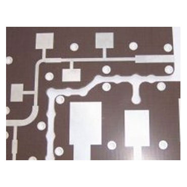
Material Special for RF Technology
|
|
| |
| |
1 TC600 from ARLON
2 TLX-8 from TACONIC
3 TMM6 from ROGER |
|
|
|
| |
 |
|
 |
|